- 您现在的位置:买卖IC网 > Sheet目录3753 > ATMEGA169P-16MCHR (Atmel)MCU AVR 16KB FLASH 16MHZ 64-VQFN
PIC16F946
DS41265A-page 186
Preliminary
2005 Microchip Technology Inc.
15.2
Compare Mode
In Compare mode, the 16-bit CCPR1 register value is
constantly compared against the TMR1 register pair
value.
When
a
match
occurs,
the
RC5/T1CKI/CCP1/SEG10 pin is:
Driven high
Driven low
Remains unchanged
The action on the pin is based on the value of control
bits CCP1M<3:0> (CCP1CON<3:0>). At the same
time, interrupt flag bit CCP1IF is set.
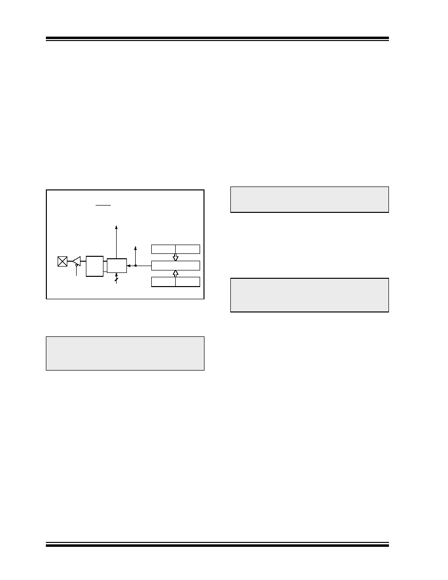
FIGURE 15-4:
COMPARE MODE
OPERATION BLOCK
DIAGRAM
15.2.1
CCP PIN CONFIGURATION
The user must configure the RC5/T1CKI/CCP1/SEG10
pin as an output by clearing the TRISC<5> bit.
15.2.2
TIMER1 MODE SELECTION
Timer1 must be running in Timer mode, or Synchro-
nized Counter mode, if the CCP module is using the
compare feature. In Asynchronous Counter mode, the
compare operation may not work.
15.2.3
SOFTWARE INTERRUPT MODE
When Generate Software Interrupt mode is chosen, the
RC5/T1CKI/CCP1/SEG10 pin is not affected. The
CCPIF bit is set, causing a CCP interrupt (if enabled).
15.2.4
SPECIAL EVENT TRIGGER
In this mode, an internal hardware trigger is generated,
which may be used to initiate an action.
The special event trigger output of CCP1 resets the
TMR1 register pair. This allows the CCPR1 register to
effectively be a 16-bit programmable period register for
Timer1.
The special event trigger output of CCP2 resets the
TMR1 register pair and starts an A/D conversion (if the
A/D module is enabled).
15.3
PWM Mode (PWM)
In Pulse-Width Modulation mode, the CCPx pin pro-
duces up to a 10-bit resolution PWM output. Since the
RC5/T1CKI/CCP1/SEG10 pin is multiplexed with the
PORTC data latch, the TRISC<5> bit must be cleared
to make the RC5/T1CKI/CCP1/SEG10 pin an output.
Figure 15-5 shows a simplified block diagram of the
CCP module in PWM mode.
For a step-by-step procedure on how to set up the CCP
module for PWM operation, see Section 15.3.3
Note:
Clearing the CCP1CON register will force
the RC5/T1CKI/CCP1/SEG10 compare
output latch to the default low level. This is
not the PORTC I/O data latch.
CCPR1H CCPR1L
TMR1H
TMR1L
Comparator
QS
R
Output
Logic
Special Event Trigger
Set Flag bit CCP1IF
(PIR1<2>)
Match
RC5/T1CKI/
TRISC<5>
CCP1CON<3:0>
Mode Select
Output Enable
pin
Special event trigger will:
reset Timer1, but not set interrupt flag bit TMR1IF (PIR1<0>),
and set bit GO/DONE (ADCON0<2>).
CCP1/SEG10
Note:
The
special
event
trigger
from
the
CCP1and CCP2 modules will not set inter-
rupt flag bit TMR1IF (PIR1<0>).
Note:
Clearing the CCP1CON register will force
the CCP1 PWM output latch to the default
low level. This is not the PORTC I/O data
latch.
发布紧急采购,3分钟左右您将得到回复。
相关PDF资料
2-1546217-0
TERM BLK RCPT 20POS SIDE 5.08MM
1-1546217-9
TERM BLK RCPT 19POS SIDE 5.08MM
1-1546217-8
TERM BLK RCPT 18POS SIDE 5.08MM
1-1546217-7
TERM BLK RCPT 17POS SIDE 5.08MM
1-1546217-6
TERM BLK RCPT 16POS SIDE 5.08MM
1-1546217-5
TERM BLK RCPT 15POS SIDE 5.08MM
1-1546217-4
TERM BLK RCPT 14POS SIDE 5.08MM
1-1546217-3
TERM BLK RCPT 13POS SIDE 5.08MM
相关代理商/技术参数
ATMEGA169P-16MCU
功能描述:8位微控制器 -MCU AVR 16KB, 512B EE 16MHz 1KB SRAM, 5V
RoHS:否 制造商:Silicon Labs 核心:8051 处理器系列:C8051F39x 数据总线宽度:8 bit 最大时钟频率:50 MHz 程序存储器大小:16 KB 数据 RAM 大小:1 KB 片上 ADC:Yes 工作电源电压:1.8 V to 3.6 V 工作温度范围:- 40 C to + 105 C 封装 / 箱体:QFN-20 安装风格:SMD/SMT
ATMEGA169P-16MU
功能描述:8位微控制器 -MCU AVR 16K FLASH 512B EE 1K SRAM LCD ADC RoHS:否 制造商:Silicon Labs 核心:8051 处理器系列:C8051F39x 数据总线宽度:8 bit 最大时钟频率:50 MHz 程序存储器大小:16 KB 数据 RAM 大小:1 KB 片上 ADC:Yes 工作电源电压:1.8 V to 3.6 V 工作温度范围:- 40 C to + 105 C 封装 / 箱体:QFN-20 安装风格:SMD/SMT
ATMEGA169P-16MU SL383
制造商:Atmel Corporation 功能描述:MCU 8BIT ATMEGA RISC 16KB FLASH 3.3V/5V 64PIN MLF - Tape and Reel
ATMEGA169P-16MUR
功能描述:8位微控制器 -MCU AVR LCD 16KB FLSH EE 512B 1KB SRAM-16MHZ RoHS:否 制造商:Silicon Labs 核心:8051 处理器系列:C8051F39x 数据总线宽度:8 bit 最大时钟频率:50 MHz 程序存储器大小:16 KB 数据 RAM 大小:1 KB 片上 ADC:Yes 工作电源电压:1.8 V to 3.6 V 工作温度范围:- 40 C to + 105 C 封装 / 箱体:QFN-20 安装风格:SMD/SMT
ATMEGA169P-8AU
制造商:ATMEL 制造商全称:ATMEL Corporation 功能描述:Microcontroller with 16K Bytes In-System Programmable Flash
ATMEGA169P-8MU
制造商:ATMEL 制造商全称:ATMEL Corporation 功能描述:Microcontroller with 16K Bytes In-System Programmable Flash
ATMEGA169PA
制造商:ATMEL 制造商全称:ATMEL Corporation 功能描述:8-bit Microcontroller with 16K Bytes In-System Programmable Flash
ATMEGA169PA_1
制造商:ATMEL 制造商全称:ATMEL Corporation 功能描述:High Endurance Non-volatile Memory segments